Test and Measurement Technology
Semiconductor manufacturing depends on reliable dimensional, film, surface, defect, and process measurements. Review how metrology supports useful production decisions.
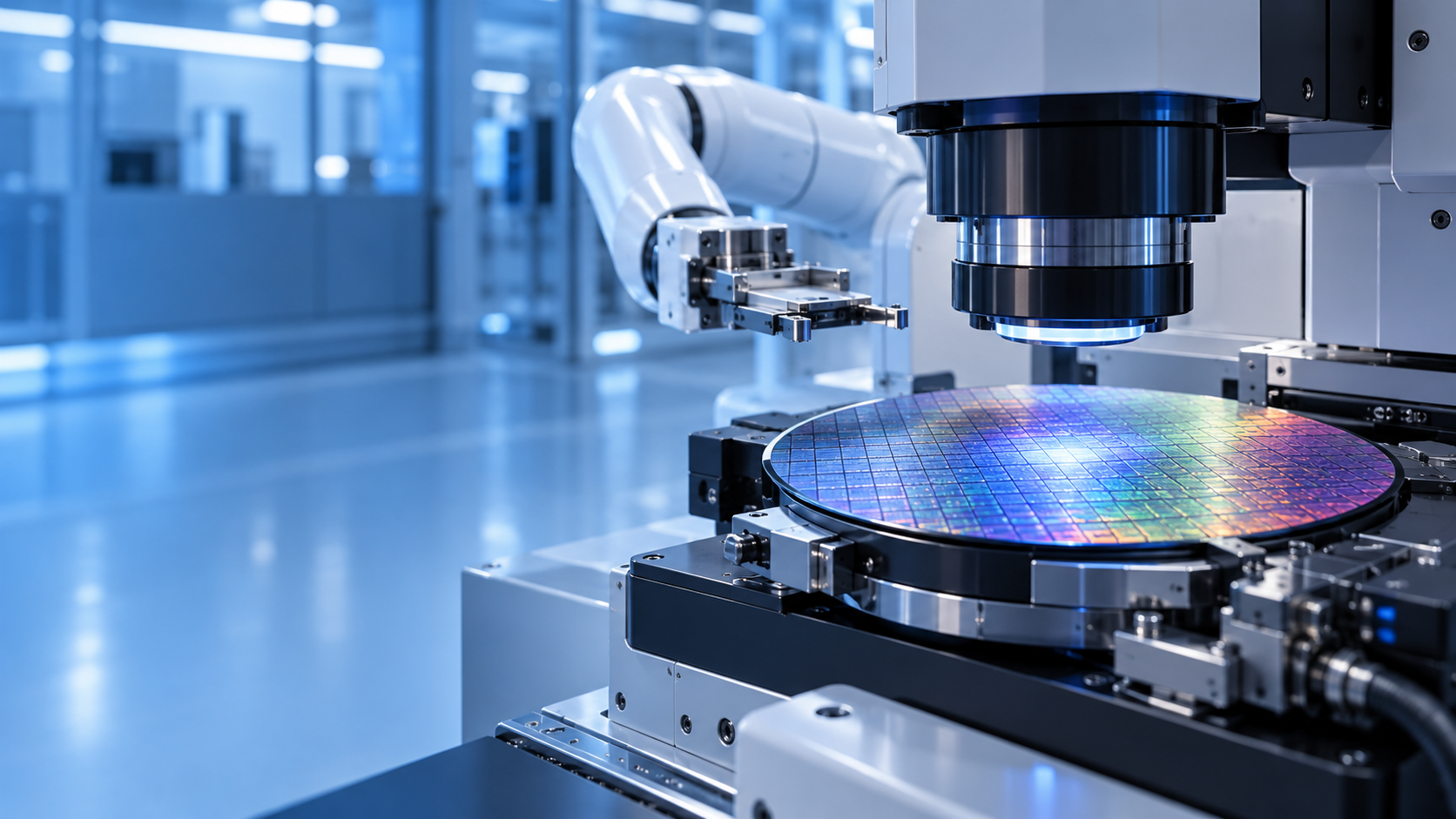
Modern electronics depend on semiconductor devices manufactured with extraordinary precision.
As semiconductor features become smaller and manufacturing processes become more complex, one thing becomes increasingly important: accurate measurement.
This is where advanced metrology plays a critical role.
Semiconductor manufacturing involves many complex stages, from wafer processing and thin-film deposition to lithography, inspection, testing, and final quality control.
At every stage, manufacturers need reliable measurement data.
Wafer metrology helps manufacturers understand thickness, uniformity, surface characteristics, dimensions, and variation across the wafer.
Even a small change in measurement can provide important information about the manufacturing process.
Semiconductor devices also contain extremely thin layers and incredibly small structures.
Advanced metrology helps engineers measure these layers and determine whether the manufacturing process is producing the required results.
Lithography is another area where precision is essential.
Lithography creates the tiny patterns that form semiconductor structures.
As these features become smaller, measuring critical dimensions becomes increasingly important.
Manufacturers also need to detect defects.
Advanced inspection systems can identify particles, surface defects, pattern problems, and other abnormalities that could affect semiconductor performance.
But measurement becomes even more powerful when it is connected to process control.
Engineers can compare measurement results with equipment conditions, process parameters, and production history.
This helps them identify changes and investigate possible causes.
Modern semiconductor factories generate enormous amounts of measurement data.
Advanced analytics can examine this information across wafers, equipment, processes, and production history.
Artificial intelligence can add another layer of analysis.
AI can identify unusual patterns, compare current measurements with historical behavior, and help engineers prioritize areas that need investigation.
But an AI warning is not a diagnosis.
An unusual measurement pattern can have many possible causes.
Engineers still need to investigate the equipment, process conditions, materials, environmental factors, and measurement system.
This is why engineering judgment remains essential.
Reliable AI analysis also depends on reliable measurement data.
Calibration, traceability, measurement procedures, uncertainty, and data quality remain fundamental parts of semiconductor manufacturing.
Advanced metrology does not replace measurement discipline.
It strengthens it by giving manufacturers better information about what is happening inside their processes.
The basic concept is simple:
Measure accurately.
Validate the data.
Analyze the information.
Investigate the results.
Then take the appropriate engineering action.
As semiconductor technology continues to advance, manufacturing processes will become even more demanding.
Features will become smaller.
Processes will become more complex.
And the amount of measurement data will continue to grow.
Advanced metrology gives manufacturers the tools to understand this complexity.
It can help control variation, improve process understanding, detect problems earlier, support quality control, and improve manufacturing decisions.
The future of semiconductor manufacturing is not AI but instead metrology.
It is AI working together with advanced metrology, reliable measurement systems, and experienced engineers.
Because better semiconductor technology starts with better measurement.
Measure precisely.
Control processes.
Improve manufacturing.
Comments
Post a Comment